

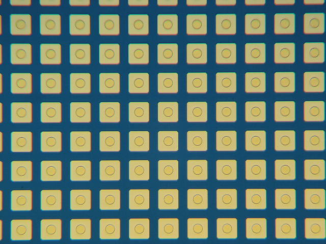
Patterned electrode
Our photolithography technique enables to form patterned electrodes.
Please feel free to contact us about 1D/2D detector.
Electrode design rules for basic patterns
Pixel electrodes
●Pitch: 55μm or more
●Size: 40μm or more
●Gap: 15μm or more
●Size: 40μm or more
●Gap: 15μm or more
Strip electrodes
●Width: 40μm or more
●Gap between electrodes: 35μm or more
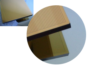
Basic Electrode Types
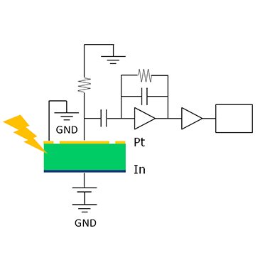 In Schottky detectors
Low dark current, hole collection
(-) pixel Pt/CdTe/In/Ti (+)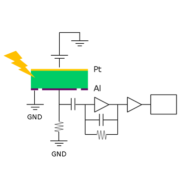 Al Schottky detectors
Low dark current, electron collection
(+) pixel Au/Ti/Al/CdTe/Pt/(-)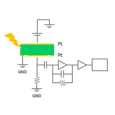 Pt Ohmic detectors
Continuously stable, electron collection
(+) pixel Pt/CdTe/Pt (-)
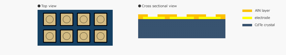
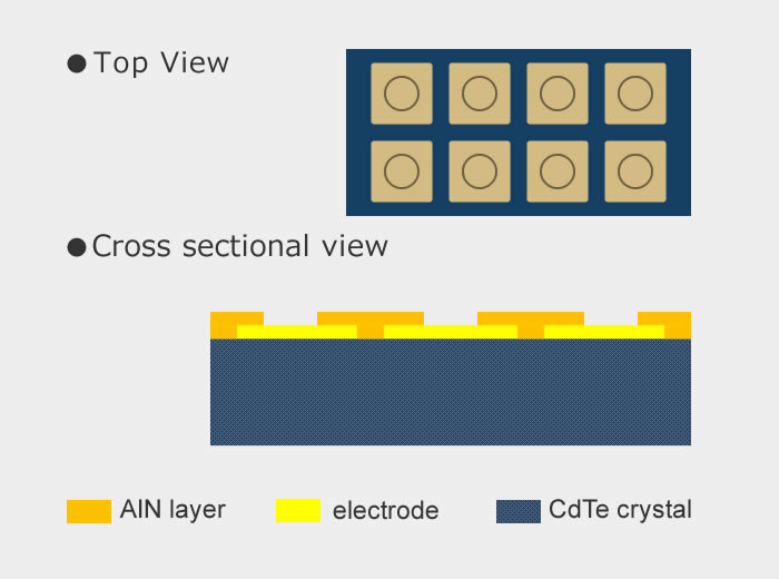
We enable to form pixel electrodes with Au layer or Au/Ni/Au layers. Please contact us if there is anything we can do for you when you place an order.
We also offer to process AIN layer on pixel electrode side to prevent solder bumps from contacting to CdTe detector surface when bonding.
CONTACT
098-934-8960
【open】8:30-17:30
[except Saturday, Sunday and public holidays]
[except Saturday, Sunday and public holidays]