

Technology
CdTe Technology Introduction Movies

About CdTe Radiation Detector
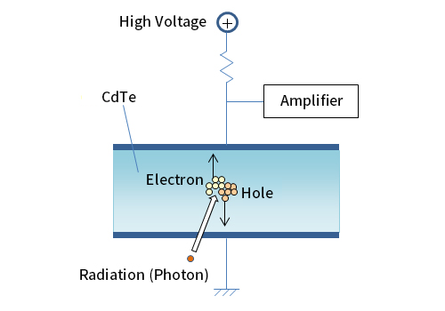
CdTe (Cadmium Telluride) is compound semiconductor formed from Cadmium and Tellurium. Bias voltage is applied to the electrodes which are formed on the both end
of high resistive CdTe wafer.
Electrical current scarcely flows when radiation is not irradiated due to the high electric resistivity; however, when radiation such as X-ray and γ- ray are exposed to
CdTe detector, they are absorbed in CdTe and electron-hole pairs are generated in CdTe. These electrons and holes are drifted to anode and cathode electrode,
respectively, by the internal electric field.
As mentioned above, radiation is absorbed in CdTe single crystal and obtained as electrical signals; this is the operation principle of CdTe radiation detector.
High Detection Sensitivity
To detect radiation such as X-ray and γ-ray, it is required that exposed radiation is absorbed and electron-hole pairs are created.
If radiation isn’t absorbed and transmits through the crystal, the radiation cannot be detected. Thus, radiation detector requires to be made of materials which have high absorbency to detect radiation.
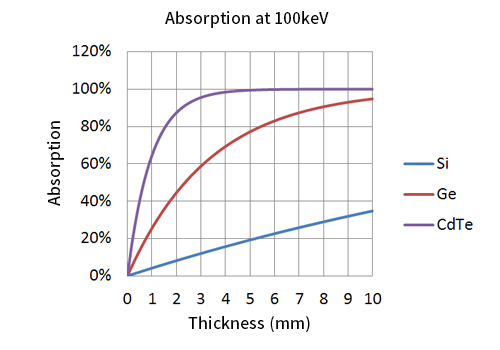
The higher level of radiation absorption is, the larger atomic number of material is. It is the reason lead (Pb: atomic number is 82) is used to shield X-ray.
Atomic number of Si (Silicon) is 14 and Ge (Germanium) is 32, which have been traditionally utilized as semiconductor radiation detector. On the contrary, effective atomic number of CdTe is 50 and it has much larger radiation absorbency compared to Si and Ge radiation detectors, which means that CdTe detection sensitivity is very high.
The right graph shows absorption rate by detector thickness of Si, Ge, and CdTe when applying 100kev X-ray. Absorption of CdTe is much higher than Si and Ge, and it is greatly expected that the thin detector bears high sensitivity.
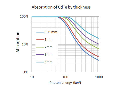
The right graph shows radiation energy absorbency of CdTe detector by thickness. X-ray energy used in medical and non-destructive inspection equipments is 200keV or lower in most cases, but CdTe has sufficient sensitivity with some mm thickness.
High detection sensitivity of radiation detector has profound meaning in medical application; higher sensitivity a sensor has, lower radiation exposure for use and less radiation dose to patients become. Also the measurement time can be reduced.
High Energy Resolution
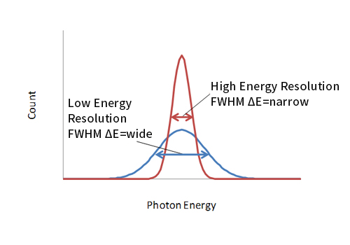
Radiation such as X-ray and γ-ray are “ray” but they are in fact particles possessing energy, called “photons.” As electric charge generated is proportional to photon energy absorbed into crystal, photon energy can be determined by measuring the induced charge.
Electric charge generated in crystal, however, sometimes cannot reach to electrodes due to recombination and being trapped by impurity level during its transmission. This leads the measured energy varies in certain degree even the photons with the same energy are irradiated; small variation of the energy means the detector has high energy resolution.
Energy resolution can be determined by a width of spectrum with full width at half maximum (FWHM) through measuring photon energy emitted from γ-ray sources.
One of CdTe radiation detector characteristics is sufficient energy resolution applicable for various applications; the characteristic is very useful for identification of radiation nuclide for environmental inspection, material identification with X-ray fluorescence, image clarification by eliminating scattered rays at optimum energy window setting of medical gamma camera.
Room Temperature Operation
Germanium semiconductor radiation detector is known as high energy resolution radiation detector.
However, Germanium semiconductor detector needs to be cooled by, for example, liquid nitrogen to use because its band gap is small, 0.67eV, and generates much leakage current induced by heat under room temperature.
Since the detector needs to be cooled down, large equipments are required and the use in field is greatly limited.
High Spatial Resolution
Radiation technology for medical uses, non-destructive inspection, and security screening is generally applied to radiation imaging, and of course clear images with sharp outlines are demanded.
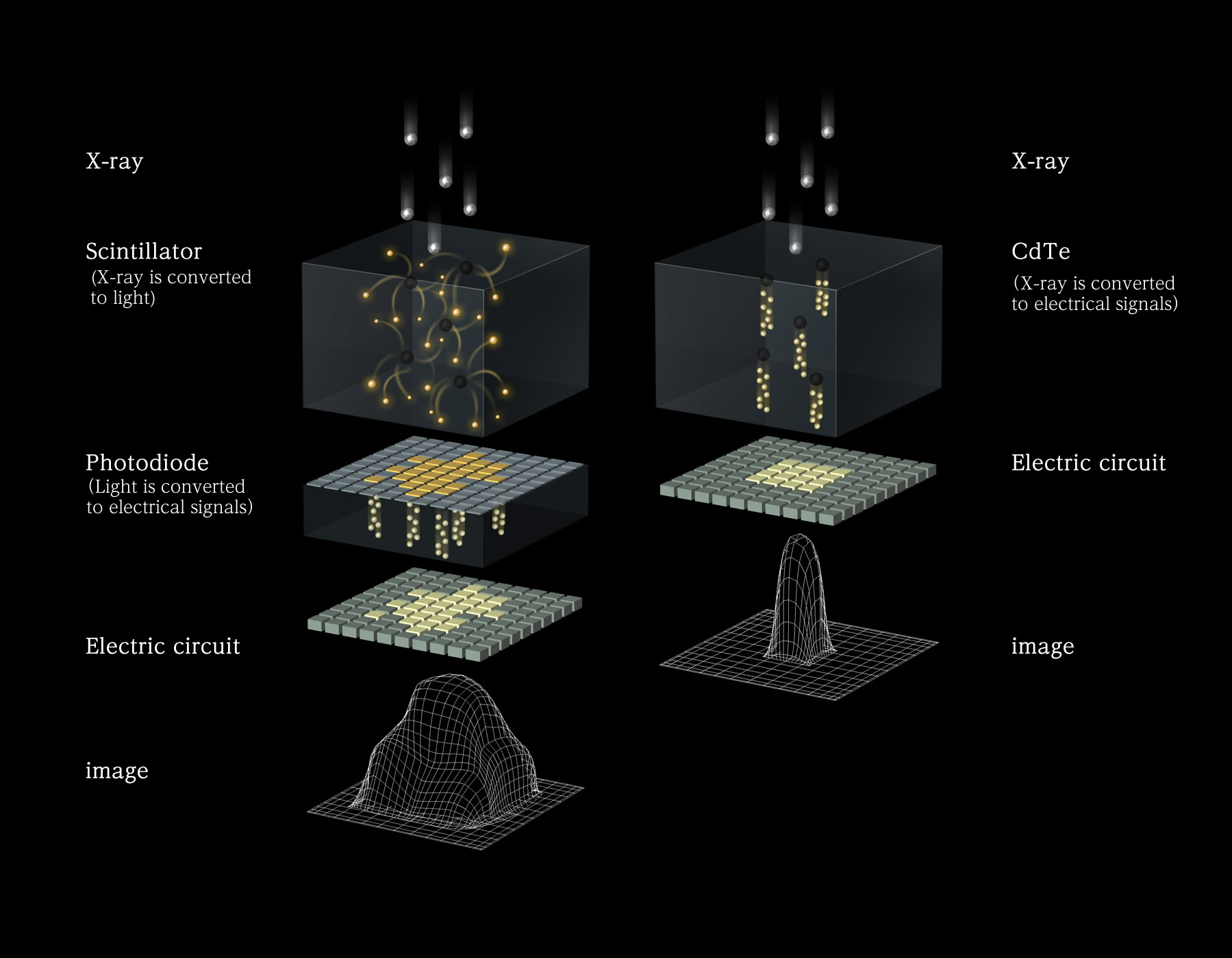
Conventional flat panel detector to obtain radiographs has a structure scintillator layer is formed on photodiode. Radiation is absorbed into the scintillator layer and converted to visible light. Photodiode detects and changes the light to electrical signals. This is called an indirect conversion detector.
The light converted from radiation via the scintillator is emitted to all directions; photodiode reacts to not only the area radiation is exposed but also the near exposed area. It makes object outlines of the radiograph unclear.
As regards CdTe detector, radiation exposed to the crystal is directly changed to electrons and holes, electric charge carrier; it is called a direct conversion detector. Electric charges generated from the absorbed radiation directly gravitates towards electric fields and is transferred to pixel electrodes. Hence, signals hardly spread over; the structure enables obtaining sharp radiographs.
[except Saturday, Sunday and public holidays]